
Offset Placement After Solder Screen-Printing
Offset Placement After Solder Screen-printing
Offset Placement After Solder Screen-printing is a complete mounter solution promoting a self-alignment effect for reducing the rate of defects after reflow caused by solder printing positioning misalignment.
Catalog download ContactWhat is “offset P;acement After Solder Screen-Printing”?
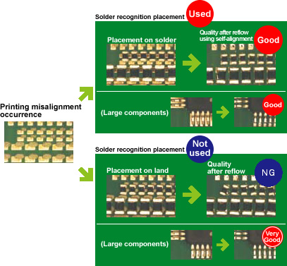
Solder printing position misalignment is caused by factors such as circuit board circuit pattern stretch and twist in different manufacturing lots. This can result in solder printing offsets during screen printing.
Particularly for smaller chip components such as 0402 (01005) and 0603 (0201) that are small in size and light in weight, the influence of solder printing position misalignment can be devastating, with the solder print sometimes more than around 30% off the pad, resulting in massive assembly defects.
Offset Placement After Solder Screen-printing can reduce or eliminate these defects through corrected placement at the solder printing positions to promote the self-alignment effect.
*Off course if the misalignment of the circuit pattern is so great that the solder print is completely off the pad, the self-alignment effect may not occur.
Realizes improvements in quality after reflow for the following types of production
- Use of very small components
- Production of two-sided mounting boards
- Production of flexible and ceramic boards
- Use of jig and matrix boards
- Production using atmospheric reflow
Features
-
Placement correction function using solder recognition
In this function, the solder printing position on the printed circuit board is detected using the camera in the mounter, and the component is given corrected placement coordinates centered on the solder. Because collective correction of target components is carried out based on several solder printed positions, the recognition time is short, and for each placement point it is possible to select either board fiducial mark recognition corrected placement as normal, or to select solder recognition corrected placement as determined by Offset Placement After Solder Screen-printing.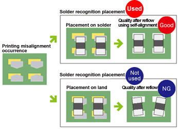
-
Offset Placement After Solder Screen-printing is the low-cost solution
In this low-cost solution, because the mounter recognizes printing misalignment and carries out corrected placement without requiring other equipment such as a solder paste inspection machine, it will be possible to simply introduce the system as it is into the line configuration and peripheral equipment that you are currently using. No additional equipment is required, so the line need not be changed.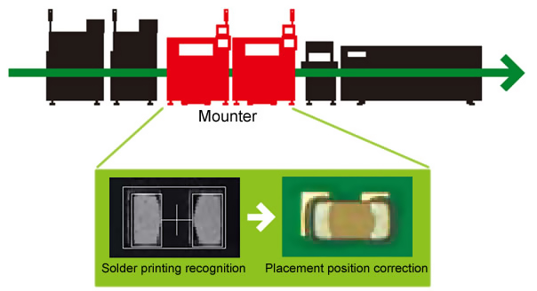
-
Reduction of recognition time in multi-panel circuits
In multi-panel circuits, by detecting the solder on the furthest away diagonal of the whole circuit board, collective correction of all circuits will be possible, allowing a great reduction of the solder recognition tact time.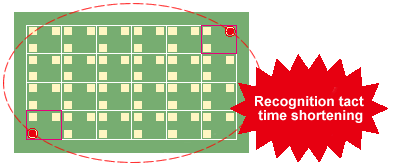
- Log Information Storing Function
It is possible to store records of the printing misalignment amounts for use as data during quality improvement.
Specifications
| Model name | Offset Placement After Solder Screen-printing |
|---|---|
| Basic Functions | ① Functions for solder printing position recognition using the mounter, and for corrected placement on the solder printing position *1 |
| ② Function for inspecting the amount of printing misalignment from a specified position | |
| Component Types | Square chips (0402 (01005) – 3216 (1206)), and 2-item single grouped symmetrical solder printed patterns |
| Circuit Board Materials *2 | Glass-epoxy, paper phenol, flexible, or ceramic boards |
| Applicable Equipment | KE-2050, KE-2060, KE-2050R, KE-2055R, KE-2060R, KE-2070, KE-2080, FX-1R, CX-1 *3 |
*1 This function allows component placement on printed paste, and does not assure equipment performance and production quality due to other material problems.
*2 The contrast between the substrate color or land color and the printed solder can be obtained using the mounter camera.
(For more details, please contact JUKI.)
*3 Please ask for the other equipments.